Delta-Delta feature is proposed in 1986 by S. Furui and Hermann Ney in 1990. It’s simply add first and second derivative of cepstrum to the feature vector. By doing that they say it can capture spectral dynamics and improve overall accuracy.
The only problem is that in a discrete signal space getting derivative from the signal increase spontaneous noise level so instead of simple first and second order derivative HTK proposed a differentiation filter. This filter basically is a convoluted low-pass filter on top of discrete signal derivative to smooth out the result and remove unwanted noises. In Fig 1 you can see the result of simple second derivative vs the proposed differentiation filter.
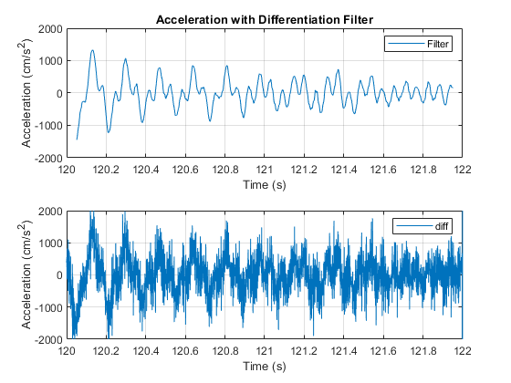
Fig. 1. Plain dervative VS differentiation filter. courtesy of Matlab™
HTK filter for a Delta-Delta feature (order=2, window=2) is a 9 element FIR filter with following coefficient(Θ is window size which is 2 in HTK)

| • Reverberation: | Is the effect of sound bouncing the walls and getting back in a room. The time is roughly between 1 and 2 second in an ordinary room. You can use Sabine equation to do more accurate calculation. |
compressor filter in speech instead of CMVN to normalize in real-time.IEEE ICASSP ’86 – Isolated Word Recognition Based on Emphasized Spectral Dynamics
IEEE ICASSP ’90 – Experiments on mixture-density phoneme-modelling for 1000-word DARPA task
Desh Raj Blog – Award-winning classic papers in ML and NLP
| • Lattices: | Are a graph containing states(nodes) and arcs(edges). which each state represent one 10ms frame |
| • Arcs: | Are start from one state to another state. Each state arcs can be accessed with arc iterator and arcs only retain their next state. each arcs have weight and input and output label. |
| • States: | Are simple decimal number starting from lat.Start(). and goes up to lat.NumStates(). Most of the time start is 0 |
| • Topological Sort: | An FST is topological sorted if the FST can be laid out on a horizontal axis and no arc direction would be from right to left |
| • Note 1: | You can get max state with lat.NumStates() |
| • Note 2: | You can prune lattices by creating dead end path. Dead end path is a path that’s not get end up to the final state. After that fst::connect will trim the FST and get rid of these dead paths |
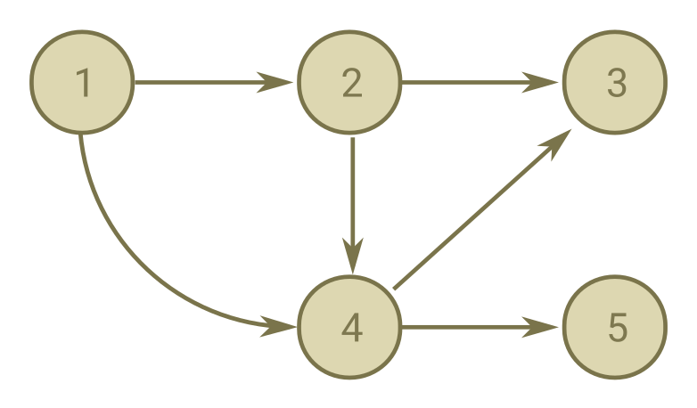
Fig. 1. Topologically Sorted Graph
| • Link: | Same as arc |
| • Token: | Are same as state. They have costs |
| • FrameToks: | A link list that contain all tokens in a single frame |
| • Adaptive Beam: | Used in pruning before creating lattice and through decoding |
| • NEmitting Tokens: | Non Emitting Tokens or NEmitting Tokens are tokens that generate from emitting token in the same frame and have input label = 0 and have acoustic_cost = 0 |
| • Emitting Tokens: | Emitting Tokens are tokens that surpass from a frame to another frame |
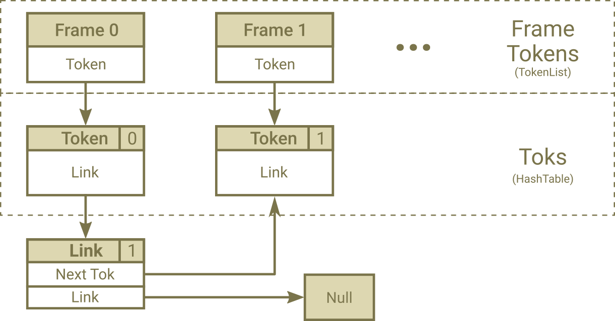
Fig. 1. After First Emitting Nodes Process
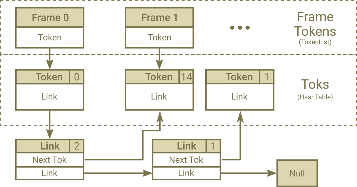
Fig. 2. After Second Emitting Nodes Process
A Simplified Block Diagram of ASR Process in Kaldi

| • Costs: | Are Log Negative Probability, so a higher cost means lower probability. |
| • Frame: | Each 10ms of audio that using MFCC turned into a fixed size vector called a frame. |
| • Beam: | Cutoff would be Best Cost–Beam (Around 10 to 16) |
| • Cutoff: | The maximum cost that all cost higher than this value will not be processed and removed. |
| • Epsilon: | The zero label in FST are called <eps> |
| • Lattices: | Are the same as FSTs, instead each token keeps in a framed based array calledframe_toks. In This way the distance in time between each token will be perceived too. |
| • Rescoring: | A language model scoring system that applied after final state to improve final result by using stronger LM model than n-gram. |
| • HCLG(FST): | The main FST used in the decoding. The iLabel in this FST is TransitionIDs. |
| • Model(MDL): | A model that used to convert sound into acoustic cost and TransitionIDs. |
| • TransitionIDs: | A number that contain information about state and corresponding PDF id. |
| • Emiting States: | States that have pdfs associated with them and emit phoneme. In other word states that have their ilabel is not zero |
| • Bakis Model: | Is a HMM that state transitions proceed from left to right. In a Bakis HMM, no transitions go from a higher-numbered state to a lower-numbered state. |
| • Max Active: | Uses to calculate cutoff to determince maximum number of tokens that will be processed inside emitting process. |
| • Graph Cost: | is a sum of the LM cost, the (weighted) transition probabilities, and any pronunciation cost. |
| • Acoustic Cost: | Cost that is got from the decodable object. |
| • Acoustic Scale: | A floating number that multiply in all Log Likelihood (inside the decodable object). |
 Fig. 1. Demonstration of Finite State Automata vs Lattices, Courtesy of Peter F. Brown
The command below generates a tone signal out of the speaker and receives it back through the mic. Measuring the phase diff will reveal the round-trip latency.
alsa_delay hw:1,0 hw:0,0 44100 256 2 1 1
Here hw:1,0 refer to the recording device that can be retrieved from arecord -l and hw:0,0 refer to the playback device. Again can be retrieved from aplay -l .
The 44100 is the sampling rate. 256 is the buffer size. 256 works best for me. Lower numbers corrupt the test and higher numbers just bring more latency to the table. Don’t know exactly what nfrags input and output arguments are but 2 1 and 1 respectively works magically for me. I just tinkering around and found these numbers. No other number works for me.
1. Focusrite Scarlett Solo Latency: 2.5ms
2. Shure SM57 Mic Latency: 2.5ms
3. OverAll Delay: 14ms with non-RT mode
You can tinker around the effect of latency with
pactl load-module module-loopback latency_msec=15
To end the loopback mode
pactl unload-module module-loopback
As Always Useful links
Arun Raghavan – Beamforming in PulseAudio
Arch Linux Wiki – Professional Audio, Realtime kernel
Let’s Enhance Kaldi, Here are some links along the way. Look like YouTube is progressing a lot during the last couple of years so basically here is just a bunch of random videos creating my favorite playlist to learn all the cool stuff under the Kaldi’s hood.
LattceFasterDecoderLattices: A more complex form of FST‘s, The first version decoders were based on FST’s (like faster-decoder and online decoders). For Minimum Bayesian Risk Calculation Using Lattices will give you a better paved wayfaster-decoder: Old decoder, very simple to understand how decoding process is donelattice-faster-decoder: general decoder, same as faster-decoder but output lattices instead of FSTsDecodableInterface: An interface that connects decoder to the features. decoder uses this Decodable object to pull CMVN features from it.BestPath: An FST that constructed from the Best Path (path with maximum likelihood) in the decoded FST.nBestPath: An FST constructed from the top N Best Path in the decoded FST.GetLinearSymbolSequence: The final step in the recognition process, get a BestPath FST or Lattice and output the recognized words with the path weight. CompactLattices need to be converted using ConvertLatticeStrongly Connected Component: A set that all components are accessible (in two ways) by it’s member.ProcessEmitting that pulls loglikelihood from the decodable objectThanks to this marvelous framework, a trained model is at disposal with WER of absolute zero percent over the 10 minutes of continuous speech file. The final piece to this puzzle would be implementing a semi-online decoding tool using GStreamer. As always useful links for further inspection
gst_caps_to_string(caps)On the way to develop a driver for Scarlet Solo Gen3 to harness the power of Shure SM57 Dynamic Microphone.
Useful links to preserve:
Microsoft – Universal Audio Architecture: Guideline to for Sound Card Without Propriety Driver
Update 1: Finished developing! Here is the link to the released driver
GitHub – BijanBina/BAudio Windows 7 x64
So the third year has been passed. I mostly worked on developing a couple of hardware projects. Halsey music was a big passion there.
Learning all ML cool stuff now is one of my top priority. Combine it with the emerge of Talon, a powerful C2 grammar framework by Ryan Hileman, and wave2letter a game-changing speech recognition engine from the Facebook AI department, I have some hope to make distinct progress.
Watching Emily Shea demonstrating how she uses Talon to write Perl was a big improvement over the past few years. And then Ryan last week’s tweet: .
Conformer better handles accents as well as fast speech. Here's a demo dictating Vue code
at high speed with the new model, with no errors. Compared to two typists on the same code:
80wpm typist took 1m54s, 120wpm took 53s. It took me 1m15s with voice. I think I could go faster!

— Ryan Hileman (@lunixbochs) April 3, 2021
This month also Microsoft bought Nuance for $19.7 billion, This will be Microsoft’s second-biggest deal ever. Now the industry is going to see a tremendous change in the SR area.
YouTube – PyGotham 2018:Coding by Voice with Dragonfly
GitHub – AccJoon: MSAA-Based Tool to Access Any Control in Win32
GitHub – Rebound: Control Linux and Windows with remote XBox-One Controller
Google Cloud Platform Podcast – Voice Coding with Emily Shea and Ryan Hileman
TheRegister – Microsoft acquires Nuance—makers of Dragon—for $19.7 billion
YouTube – Halsey: Nightmare (Live From The Armory)


