One of the great feature that comes along with ADS Package is the ability to create your design in a reverse flow. This necessity become more evident when you prefer to use other feature-reach layout tool than ADS and use ODB++ or ADFI tools afterward to import the design into the ADS for performing layout verification. In this tutorial I will summarize multitude of notes that you should consider to get a successful schematic back from your designed layout.
To start, first convert the traces into microstrip transmission line by right clicking on a trace and select Path/Trace > Convert Traces. If you were lucky the trace would change to microstrip type without any significance change in the trace color but if that’s not the case, you’ll notice changes in trace appearance like becoming invisible or transportation into a wrong layer. This is illustrated in Fig. 1 that shows a transformation nullify the line due to the fact that new wrong layer is an outline type. To solve the issue, proceed to the following steps. In case you hadn’t counter to the mentioned problem you can skip following steps abd generate schematic directly by Schematic > Generate/Update Schematic in the layout window.
Fig. 1. Transform the trace to microstrip will change the layer unwillingly
ADS sometimes have issues with ports and terms. So if you cannot generate schematic from the layout it is probably the main cause.
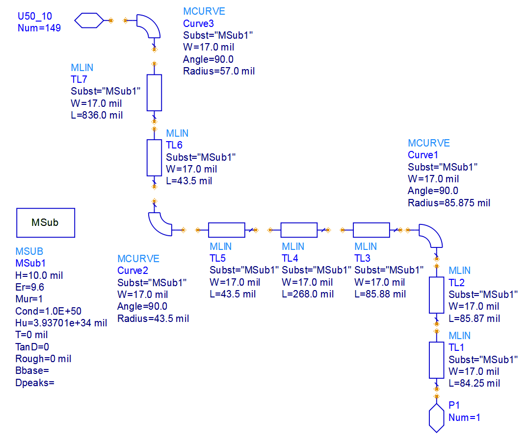
After generating schematic you’ll notice unconnected components placed vertically on the canvas. If you rearrange the components you get something like Fig 2 which by now you were recognized that ADS failed to import the connectivity back into the schematic. Unfortunately there is no automated fixation for this issue, which leaves you with no option but to make the connections manually. After that from the Parts panel, add a MSub component into the canvas. Now if you checkout files in your workspace you witness a new file named tech.subst. This file is a auto-generated stackup file that in many cases may contain some errors so it it recommended to to compare new generated substrate file with your current stackup and apply the required changes.
The last step is to configure the layer that microstrip will land on. To do so, double click on MSub component and adjust Cond1 parameter. Cond2 is, ADS said and I quote
Layer on which the air bridges will be draws
Probably the ground layer but still I have a doubt about that. Finally by selecting Layout > Generate/Update Layout in the schematic window regenerate the layout.
Cheers!


