ADS has a broad way of aspects from IC design to the RF simulation, here we explore how to prepare your workspace to start layout phase after schematic design. ADS comes with tons of ready to use parts, these parts are available at <ADS>/ADS/oalibs/componentLib/. Here I demonstrate how to add and use RF_Passive_SMT library in your layout.
DesignKits>Unzip Design Kit...<ADS>/ADS/oalibs/componentLib/ and select library filebefore using the parts you need to setup the substrate file and technology file.
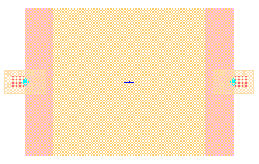
Options>Technology>Technology Setup.Referenced Libraries click on Add Referenced Library... button.ads_standard_layers and click on Ok button.Technology Setup dialogue and setup your substrate file based on ads_standard _layers that you imported earlierThe below image shows fooprint of ATC cap that inserted into layout.

To create footprint(artwork), you have two options:
1. create the layout by inserting rectangle, traces and etc into the board by using layout editor. In the reference links you can find link of an YouTube video demostrating that.
2. write an AEL script to create the artwork for you.
First option is easy, fast and works out of the box but it’s not scalable. writing down an AEL function is more clean from designer point of view. Fortunately Dr. Mühlhaus company wrote down a comprehensive guide (link down below) on how to create an Artwork based on AEL language.
Useful Links
YouTube – A vs B Modeling and Layout Footprint Generation