Inserting via in RF and Microwave regions might seems to be a scary thing to do but as revealed through EM simulation for low portion of Microwave frequencies (below 10GHz) using a full via isn’t as worse as it seems to be. From “full via” I mean a via that start from top layer and end in bottom layer, using a partial via (that end or start on layers other than top or bottom) will results in considerable amount of reflection and poor S11.
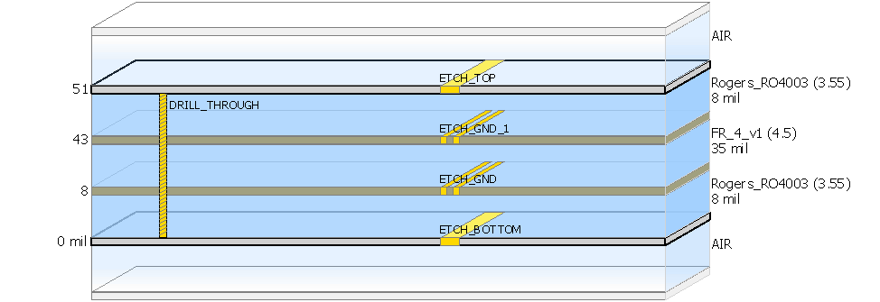
In order to find out a perfect transition from the top layer to the bottom layer , I use ADS Via Designer tool, to sweep on all available parameters. I ran parameter sweep on Drill Diameter, Anti-Pad diameter and pad size. I used a simplified stackup shown below which is a typical stackup in may RF boards, two layers of 8mils RO4003 substrate around a FR4 prepreg.
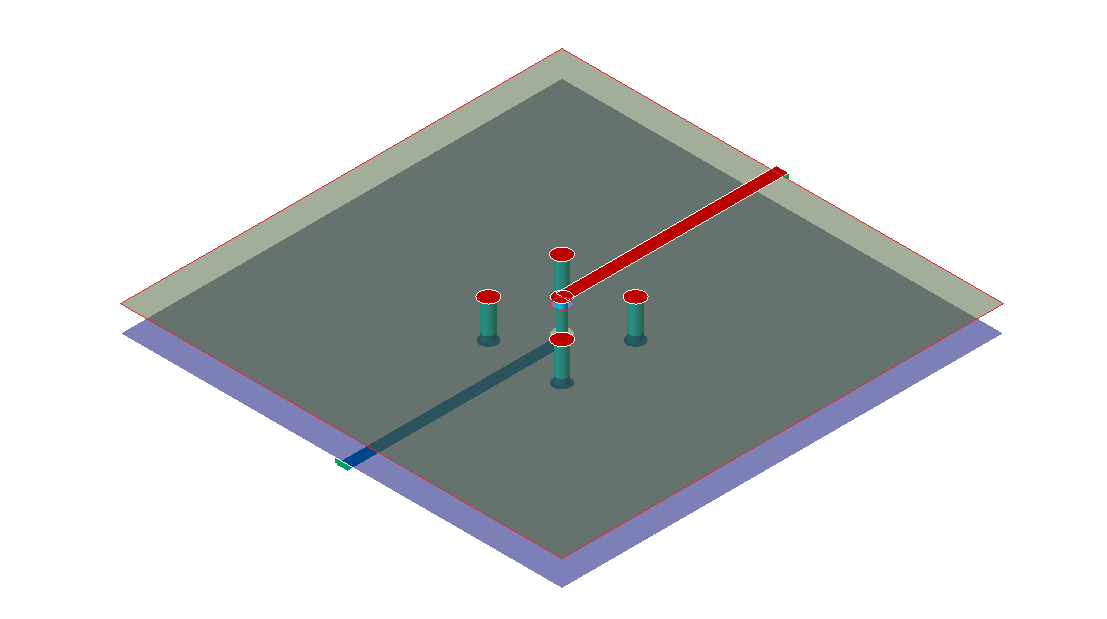
One of the main concerns regarding designing a perfect Via structure is being careful about return current path. In the case of my design, because I used GCPW (grounded coplanar waveguide) a rectangular via stitching may integrate more naturally to the board, albeit a two horizontal may work out too. On of the first concern in selecting right via stitching is distance of vias. Through long simulations I figure out that the perfect result will achieve when you place transition via stitching in the same position as the stitching vias you used to construct your GCPW.
In the following design with 17mils trace width and GND guard of 16 mils from each edge of transmission line, a via stitching with 100mils distance between center-to-center of via works the best.
Note: dx and dy in ADS Via Designer are distances from the TL not from the corresponding via.
For the TL via, three degree of freedom are available but from manufacturing and physical point of view some of these values may not be practical. drill size is the most constrained parameter that restricted to both available bit size and the free space that is available on the board. After playing around these three parameters, it seems that no matter what value you choose for your drill size, there is always some pad size and anti-pad value that compensate drill size. For the pad size and anti-pad value you are limited only by the clearance value of your PCB manufacturer. For both of these value a step size of 1 mils seems to be fair. In my case I use a 0.3mm (12mils) drill size, and because of 4mils clearance the anti-pad diameter should be equal or bigger than 20mils.
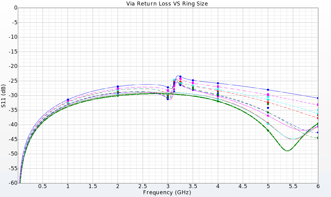
After running a lengthy sweep on via ring size and antipad diameter, it revealed that at 0.3mm drill size, the via structure shows more inductance than capacitance. To reach a perfect wideband 50Ohm characteristic impedance, adding more capacitance to the structure was a must. In compliance with simulation results, best performance achieved when via ring is large enough and antipad is shorten to it’s minimum values. In my case the final choice was 0.3mm drill size, 27mm as the diameter of via pad and 8mils(min clearance)+12mils(drill size)=20mils for antipad diameter. The thicker green line at bottom is the S11 of chosen via.
To conclude this post, we saw that at small drill sizes, DFM rules prevent to reach a decent performance. Small drill sizes results in higher inductance that need to be compensated by tight GND coupling and large via pad. To surpass this drill sizes can be choose to be bigger resulting in lower inductance and relieving capacitance requirement. Designing a via at low frequencies (sub 6GHz) isn’t a challenging problem but getting an invisible via from EM point, can be a big thumbs up work to do, moreover same rules and workflow can be applied at more critical frequencies to achieve better performances.


